- Preamplifier PCB on OSH Park
- Preamplifier PCB Eagle files
- Analog PCB schematics
- Analog PCB gerber files
- Analog PCB Altium Designer files
Circuit overview
The STM electronics work like this: a microcontroller (Teensy 3.1) scans the tip in a raster pattern by generating X and Y scanning signals using a DAC. A DC bias voltage, also generated by a DAC, is applied to a conductive sample, causing electrons to tunnel across the gap between the tip and the sample when they are brought close enough together (<1 nm). This current is measured by a preamplifier, which outputs a voltage proportional to the tunneling current. This signal is digitized and fed into a PI control loop, the output of which is sent to a DAC and used to drive the scanner’s Z-axis, causing the tip to track the sample topography. What’s truly amazing is that this actually works really well! The tunneling current increases exponentially (by around a factor of 10 per Angstrom) as the tip gets closer to the sample surface, and this is what makes the STM so sensitive, to the point of being able to resolve individual atoms under ambient conditions.
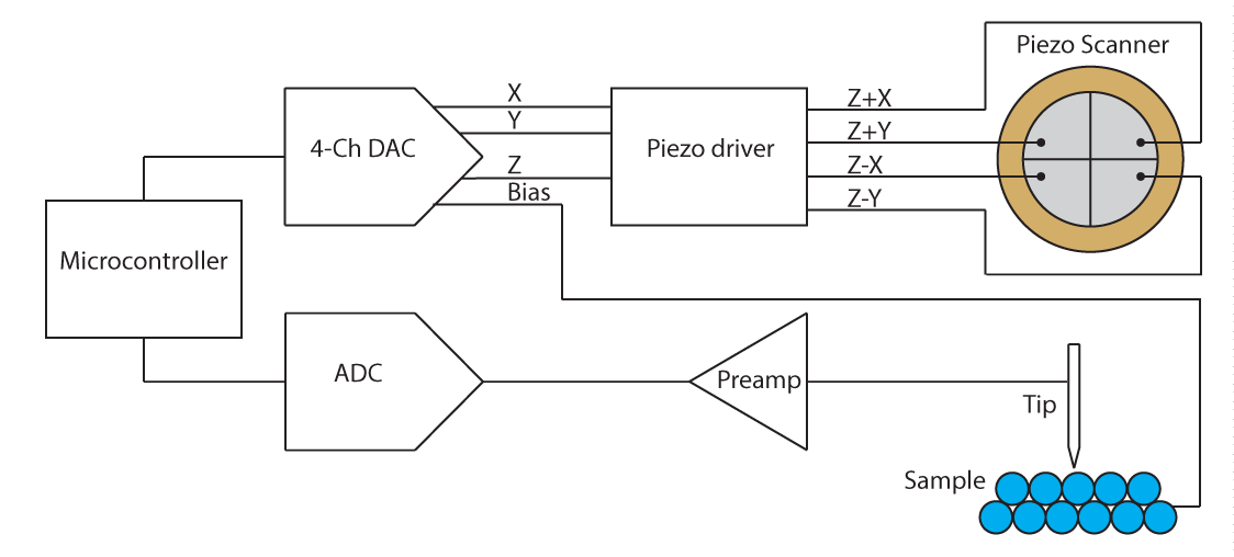
Both the input (tunneling current) and output (Z-axis) signals are sent to a PC over USB, where the images are constructed line-by-line as the scan progresses. I wrote a C# program that takes care of this, and allows me to set the various scan parameters.
The Teensy is currently installed on a piece of prototype board separate from the main analog electronics board. I plan on replacing it eventually with something faster.


Tunneling current preamplifier
The preamplifier is an OPA124 op-amp with a 100 MΩ feedback resistor configured as a transimpedance amplifier. The output voltage of the amplifier is simply the tunneling current multiplied by the value of the feedback resistor. With a 100 MΩ resistor, it can measure currents up to 100 nA. I typically operate the microscope with a setpoint around ~1 nA, but it’s important to have a couple extra orders of magnitude of range here since the tunneling current varies exponentially with tip-sample distance.
I chose the OPA124 for it’s low input bias current and low current noise. There are many others that would also work well: OPA627 seems to a popular choice in STM; OPA129 would be good for measurements at very low currents; LTC6268 has ridiculously low input bias current, but I’m not aware of anyone using it in an STM. The input bias current needs to be significantly lower than the tunneling current, or the measurement will be horribly inaccurate. OPA124 has input bias currents around 1 pA.
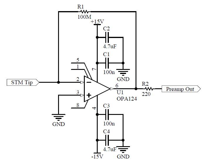
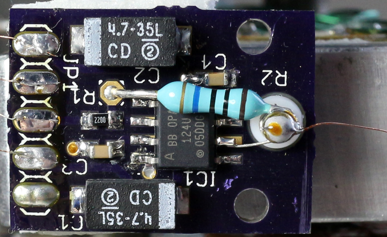
I’ve built the preamp on its own small PCB and mounted it directly on the STM head. A short 40 AWG wire connects the STM tip to the preamp input. I place a metal can over the STM during scanning to shield the tip and preamp. Without the shield, the images produced by the STM are dominated by 60 Hz noise pickup.
Since the tunneling current is pretty small, care needs to taken to avoid leakage currents. Currents leaking into the op-amp input node will be summed with the tunneling current by the preamp and create a significant offset error, so ideally we want to keep the leakage current smaller than the input bias current. This means that the preamp input node needs to be really well insulated from other conductors. I’ve insulated the input node with a teflon standoff (Keystone Electronics 11301) and bent the op-amp’s input pin off the surface of the PCB. A surface mount feedback resistor with a guard ring around the input node would probably be a better choice though, as it would result in lower parasitic capacitances and higher bandwidth. This is described in the OPA124 datasheet.
Data acquisition
Since the preamplifier is located off the main PCB, I’m taking a differential measurement to compensate for noise which might be picked up in the wiring. The preamp output and ground signals are buffered and filtered by an LT1469 dual op-amp (U12), which drives the inputs to an LTC2326-16 16-bit pseudo-differential ADC (U10).
Feedback loop
The Teensy 3.1 takes the log of the input data (since tunneling current varies exponentially with tip-sample distance) using a lookup table containing 2^16 entries, i.e. one for every possible ADC reading. The linearized signal is fed into a PI loop, which outputs the Z-piezo signal.
Scanner outputs
The Teensy outputs X, Y and Z signals via a DAC8814 4-channel 16-bit multiplying DAC. Accuracy is not particularly important here, but resolution and dynamic range are. The STM needs to be capable of tracking atomic surface features while having enough travel range to compensate for some thermal drift. The Z-axis has somewhere around ~2 µm of travel, so 1 LSB with a 16-bit DAC is ~0.05 nm. This is subatomic, but still a bit “coarse” for an STM. Ideally it should be less than 0.01 nm. One solution is to reduce the Z-axis travel range by changing some resistor values. That travel range is useful though in compensating for thermal drift, so instead I’m using sigma-delta modulation to increase the effective DAC resolution to 20-bit. This essentially means doing PWM between steps of the DAC and filtering the output with a low pass filter. This article gives a good explanation of the technique. This brings the resolution down to about 2 pm, provided the noise is kept low enough. Theoretically, the SNR of this circuit is above 120dB. However, the actual resolution achieved by my STM isn’t this good. I can resolve individual atoms easily on graphite (relatively easy because it’s an atomically-flat non-metal), but not on gold. This is probably due to some combination of: vibrations, sound, noise pickup, thermal effects, poor tip quality, DAC glitches (?), etc.
I’m using a REF102 as the DAC reference voltage. The raw ouput from the REF102 is relatively noisy, so I’m filtering it with a simple RC filter consisting of a 1k resistor (R4) and 100 uF tantalum capacitor (C1).
Piezo Driver
STM’s typically use fairly large voltages (typically around ±200 V) to drive the scanner. However, piezo buzzers like the one I’m using have relatively large travels at low voltages, so I’m using ±15 V supplies for the piezo driver. This gives around ~2 microns of travel in all axes. The X, Y and Z signals are combined by op-amps U3 and U6 to generate the Z+X, Z-X, Z+Y and Z-Y signals to drive the 4 scanner electrodes. The scanner’s brass electrode plate is connected to ground, and is used to shield the STM tip from the scan electrodes.
Power supply
I’m using standard linear regulators and a transformer to generate ±15 V, +5V and +3.3V supplies. The main STM analog PCB should be shielded from the transformer and mains wiring, so I’ve put the power supply in a separate box.
Notes on wiring and PCB construction:
Connector P5 is the power input for the main analog board, and takes ±15V, +5V and +3.3V inputs.
Currently I have the Teensy on a separate piece of prototype board so that I can upgrade it later on. Connector P1 is wired to the Teensy as follows. Make sure to cut the small jumper on the bottom of the Teensy board to separate Vin from Vusb.
All GNDs -> GND
+5V -> Vin
~CS_DAC -> Teensy pin 20
~LDAC -> pin 17
~CS_ADC -> pin 21
CNV -> pin 4
BUSY -> pin 3
MISO_ADC -> pin 12
MOSI_DAC -> pin 11
SCK_ADC and SCK_DAC -> pin 13.
Connector J1 goes to the scanner. J2 goes to the preamp. On J2, “PREAMP+” goes to the preamp output, and “PREAMP-” goes to the preamp ground. I’m using ribbon cables to connect the board to the STM. Ribbon cables are floppy and should help with vibration isolation somewhat. Stiff cables are like mechanical antennas. I’ve chosen the pinouts of these connectors so that every second conductor of the ribbon cables used to connect the board to the STM is ground.
The following components are optional: U8, U9, U11, U13, R33, P2, P3, P4. They are mostly for dI/dV spectroscopy which requires a lock-in amplifier. If you leave these components out, install 0-ohm jumpers (or just solder bridge) W1 and W2, which bypass the ADG419 switches (U9 and U13) at the ADC inputs.
Some tantalum capacitor polarities are not indicated on the PCB, so refer to the PCB photos at the top of this page if you do plan on building this board. Do not install tantalum capacitors backwards, as they could burst into flames! You could even try leaving them out entirely, as they’re probably unnecessary if you power the board from a low-noise linear supply.
I have LEDs driven by the Teensy that indicate when tunneling is established. This helps with manual coarse approach.
Updated April 14, 2017.
Previous versions of this page:
