So far I have only imaged gold and highly oriented pyrolytic graphite (HOPG) surfaces. The surface must be conductive and free of any oxide layer, which actually leaves out most metals for imaging in air. This is why STM is often performed in ultra-high vacuum.
Highly Oriented Pyrolytic Graphite
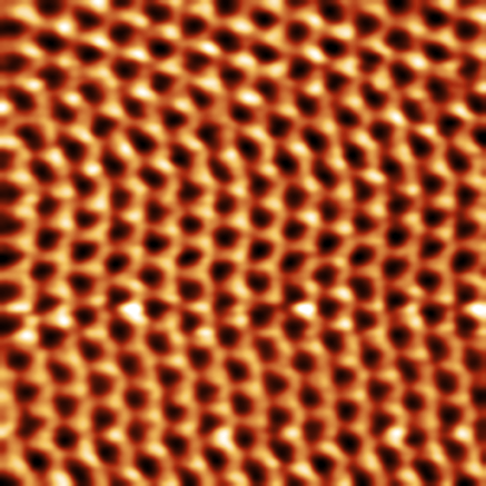
HOPG is a commonly used substrate in STM and is probably the easiest sample to obtain atomic resolution with, since it doesn’t oxidize under ambient conditions. It’s also not a metal, so it’s electrons are not delocalized all over its surface, which makes it easier to resolve the atomic structure. You can get cheap HOPG from Digikey. The image above shows the hexagonal lattice structure of HOPG. This scan was acquired in constant-height mode, but I did use a small amount of integral gain in the feedback loop to compensate for vertical drift and prevent the tip from crashing into the surface. I’ve enlarged the original scan and done some gaussian filtering to remove noise. The original scan was taken at a resolution of 128 x 128 pixels to reduce the total scan time and minimize the effects of drift on the tunneling gap. Bias voltage was 50 mV. These very small scans usually take about 0.5-5 seconds. Larger scans (100’s of nm to a few um) usually take several minutes.
Gold
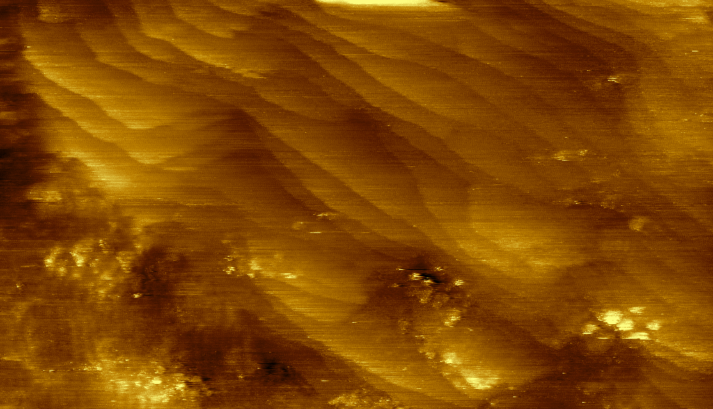
The gold surface shown above was prepared using a template-stripping technique to produce ultra-smooth surfaces, so the atomic steps are clearly visible. This image was acquired in constant-current mode with a sample bias of 50 mV and tunneling current of 1 nA. I prepared these samples as part of a project at university, and it requires a thermal evaporator, sputterer, or some other way to deposit a thin layer of gold onto a flat silicon wafer. Gold-platted electrical connectors also make great test samples.
Image Processing
I use Gwyddion to correct for vertical drift, sample tilt and scan artifacts. Gwyddion is a free, open source SPM data analysis program.
