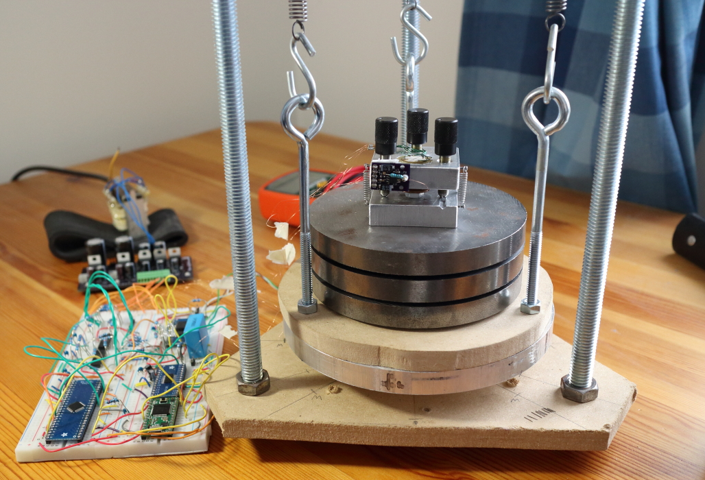
 This project is my attempt to build a low-cost scanning tunneling microscope (STM) capable of atomic resolution imaging in air. The piezo scanners typically used in STM typically cost at least hundreds of dollars. Some time ago I came across John Alexander’s simple STM project, in which he used a cheap piezo buzzer element with one of the electrodes cut into quadrants to enable XYZ motion. This type of scanner is less rigid than what is usually used for STM, but I decided to give it a try and see how far I could get with it. Turns out I was able to image highly-oriented pyrolytic graphite (HOPG) with my STM with atomic resolution! The image below shows the hexagonal lattice structure of graphite.

Overview of the technique
STM is a tool capable of imaging surfaces with atomic resolution. In STM, a sharp metallic needle is brought within a few angstroms of the surface of a conductive sample and a small bias voltage is applied across the gap. If the gap is small enough (<1 nm), electrons can cross the gap via quantum tunneling. This “tunneling current” is typically in the pA – nA range, and can be measured with a transimpedance amplifier. The STM tip is mounted on a piezoelectric scanner, which is capable of sub-angstrom motion in all directions. The tunnelling current measured by the transimpedance amplifier is fed into a feedback loop which controls the voltage applied to the Z-axis electrode of the piezo scanner and acts to maintain a constant tunneling current, and therefore a constant tip-sample distance. The X and Y axes of the scanner are used to raster scan the tip across the sample. By measuring the Z-axis voltage as a function of scan position, an image of the sample topography is constructed. If the tip moves closer to the sample surface, the tunneling current increases exponentially. This exponential relationship is what makes STM sensitive enough to resolve individual atoms, even under ambient conditions. If the STM tip is atomically sharp (not as hard to achieve as you might think!) then nearly all of the tunneling current will flow through the single atom on the tip which is closest to the sample surface, resulting in images with atomic resolution.

Hi, Dan!
I am very impressed with your project and decided to reproduce it. Unfortunately, I am not so well versed in electronics and therefore I would like to ask a question.
As I can see from one of the photos, two wires come to the bottom plate. One of them is in contact with the sample, and the second is soldered to the bottom plate. Please tell me where the second end of the wire soldered to the bottom plate is located, I can’t find it on schemes.
LikeLike
That wire is just connected to the controller ground.
LikeLike
Hi,
Great project as everybody says.
I have a question, what’s the voltage value between tip and sample during constant height scan?
LikeLike
Hi Paul,
The bias voltage really depends on the sample and isn’t any different between constant height and constant current scanning. For gold and HOPG I typically use 50 mV. A smaller voltage causes the feedback loop to move the tip closer to the sample to achieve the setpoint current. When the tip is closer to the sample the current signal is more sensitive to height changes so smaller details can be resolved.
Cheers,
Dan
LikeLike
Hi Dan,
I just wanted to tell you I have restored an archive copy of my old website that was on Geocities. I have it on GitHub now.
https://john-alexander42.github.io/simple-stm-web-page/index.htm
Even though GeoCities was closed over twelve years ago, I still get questions about that website.
John Alexander
PS I am thinking of starting a project designing an open-source SPM controller. for digital signal processing and data acquisition, I was thinking of using the Teensy 4.1 or maybe a dual-core ARM Cortex processor card with ethernet. any thoughts?
LikeLiked by 1 person
Hi John,
Great to see you’ve restored it! I’ll update my links to go to your new page.
Teensy 4.1 or some other fast ARM processor would definitely be an improvement over the Teensy 3.2 I’m using. I started a design a long time ago using an FPGA which is also a good option.
Cheers,
Dan
LikeLike
Hi Dan,
I just wanted to let you know I restored my old STM web page. I will add a link to your page shortly.
https://john-alexander42.github.io/simple-stm-web-page/index.htm
Thanks
John Alexander.
LikeLike
Hi,Dan!
I have been trying to make my own microscope in recent months until I found your website. I’m very interested in your homemade microscope and am going to make one following your example. However, your “PCB Gerber files” file link in the electronic section seems to have failed, while my level in this regard is very low. I hope you can update this link or update the Gerber file in other ways, which will be very helpful to my attempt. Thank you very much for your help!
(My English is not very good, so please forgive me if there are grammatical errors)
LikeLike
Do you mean: “STM_analog_PCB.zip”
I can show you the link that I uploaded https://www.mediafire.com/file/g7g3xwu57fhkm4p/STM_analog_PCB.zip/file
LikeLike
Thanks a lot!
Another small question is, do you know the exact model number for DAC8814 and LT1469? For example, is it DAC8814IBDBR or DAC8814ICDBR? Are they both usable?
Thanks anyway!
LikeLike
Lt1496 the difference is the working temperature as i remember.
For DAC8814 the higher price give you the high accuracy and linearity.
LikeLike
Dear Dan,
What an interesting work! I was net surfing while I was planning to make homemade AFM, and came here.
What I’m curious is that, it there any way to verify the motion of custom piezoscanner, or how to lengh-calibrate it? If I were to check individual function before the whole assembly, those sub-nano motion of piezoscanner must be imperceptible.
One way I thought of is to add a small piece of mirror and track the motion from a long distance, but if the actual motion is sub nanoscale, I will barely notice a trajectory of several micrometers within a 10 meter away or so.
LikeLike
If you had atomic resolution and could resolve HOPG or some other ‘easy’ crystalline structure, you could compare your expected xy movement with the actual moment using a literature value of the HOPG crystal lattice spacing. If you are not able to get HOPG working, you could do some other sample with a known spacing (cant thing of anything at the moment).
LikeLike
Hi Dan! Great job!
I wonder what the range of variation of the tunneling current if you set tunneling current at 1 nA under the constant height mode on HOPG.
Thanks!
LikeLike
Can this microscope be used to move atoms?
LikeLike
Disclaimer: I did not build this STM, however I work with STM for my research and I have also not tried atomic manipulation yet.
I would imagine atomic manipulation on this STM would be quite difficult. You need extremely good vibration isolation and good control over the xy motion along with a low noise readout on the tunneling current. I am not sure the op amp circuitry here is able to read those small currents with enough precision, especially without more radiation shielding. However it may be possible and all luck to you if you try it!
Cheers,
Baird Bankovic
LikeLike
1) At least I see something and it is not noise
power supply linear_PIC -> https://photos.app.goo.gl/43Bu7qtrvkjgEPfe9
– some picture shows a step – means the STM system shows something
## Note that it looks like some 60Hz noise – because the system is not good, I have minimized this 60 Hz noise
PIC-> https://photos.app.goo.gl/sMutPJjzWbjzLk326
-> when you see this picture, the left and middle picture show the same pattern, I think that the forward scan and backward scan have a drift ( or offset – I think the temperature make this) but we can say we see something that is real?
—> Dan, please tell me if my thinking is not correct ??
2) To reduce the 60hz noise above, I tried to shield the preamplifier, use 1 100Mohms resistor and it is flying with Teflon standoff.
PIC-> -> picture here https://photos.app.goo.gl/uN8owSepGMTFkknb6
I connect the shield to EARTH GROUND AND POWER GND
-> DAN AM I correct to connect the shield-like that??
3) After that I got some image https://photos.app.goo.gl/VBcUcknWY6oPqqQo8
-> Dan please evaluate the picture?
4) Some STM picture yesterday night 22 April 2021
https://photos.app.goo.gl/fKxeRAK8vbK757zY6
First, the tip is important, in the beginning, it shows that we see something, I mean some surface (see the yellow part) that don’t have 60hz noise, or it is small and make not see in the picture)
After it crashes to the mountain (see the red color), the tip is not good anymore, and we cannot see anything.
so I mean that we should make a good tip and try much time to see the atom without any filter (my thinking)
->Dan, according to these images, could you please give me some suggestions about noise or scanning? Do you think that if we make a good time, we can scan the atom-like you?
Finally, I want to say thank you for your suggestion and your help.
LikeLike
5) I use Wsxm image filtering software, assume that filter is used
https://docs.google.com/presentation/d/14_f179qu1B4AWwYUxmsdBkGptzOda5HmPZGDHlhArIw/edit?usp=sharing.
Thank you, John Alexander and Tomáš Círman for your suggestion about the linear power supply, it reduces noise 😀
LikeLike
Updated Thursday April 22 2021,
I tried to shield the system with aluminum foil (see Picture),
However, The noise still exits,
PIC -> https://photos.app.goo.gl/aSTr9Mv57h4BnHpA9
As you can see from the figure, the noise I calculated is about 30Hz (main noise) and 60Hz (double frequency). I am not sure it is correct or not.
I did use the linear power supply and shield the system (chassis connect to earth ground and power GND)
-> Please give me some hints to solve the system noise? T.T
-> I have tested more than 20 tips and still no luck . T.T
LikeLike
Dear Dan ,
if other guys have some experience or anything to ask me up to now, please contact me by minhducpham2009@gmail.com. F
This is my system so far,
SYSTEM PIC-> https://photos.app.goo.gl/Jm3rKFQhAge45KnV9
Currently, I still have some issue with software crash like ” Tomas Cirman ” and oscillation like “Vítor Barbosa”,
I can’t see any atom with STM now, but I am trying to figure out the issue.
Here is my experimental so far, hope it would help another guy,
1) It is extremely hard to approach by hand, i recommend you guy to approach using stepper motor like 2048 similar to DAN.
I use the separated external Arduino DUE to approach using serial monitor:
STEPPER MOTOR code here -> https://www.mediafire.com/file/al64moff1llbfl4/the_full_sketch_in_arduino_OK_SERIAL_STEPPER_CONTROLLER.ino/file
I use “r” for fast approach and “l” for fast retract; when the tip near the sample I use “t” and “y” for one step moving.
2) OPA 124 has a lot of oscillation and I don’t know why ? (I think it is the same issue with “Vítor Barbosa”)
In short, without filter capacitor, which is parallel with 100Mhz, the tunneling voltage measured (by pin P2 IOUT+ IOUT- ) is 0V (FLUKE multimeter), but the tunneling current LED is always turn on !!
when 1pF filter capacitor, the tunneling voltage measured (by pin P2 IOUT+ IOUT- ) is -0.4V (FLUKE multimeter) -> I think that there is some offset ?? I try simulating opa124 using TINA but this offset voltage does not appear !!
Somehow, the tunneling current LED is turned off !!
-> I think that there is a oscillation by opa 124 itself but it may not show in TINA software.
http://www.mediafire.com/folder/mackyyfl2x5k6cy,qrnv1bjbt001ff7/shared
you can see in these pictures:
opa 124 has some oscillation without filter capacitor, so that i think it is necessary to have one.
PIC OPA124 noise without CAP-> https://photos.app.goo.gl/XdVJ7Xxu4vT3B6rS6
LikeLike
I suspect your power supply. Try to use classic linear power supply. The switching noise and peaks are amplified by opearation amplifiers and mainly with bigger gain as in this preamplifier.
Tomas
LikeLiked by 2 people
Thank you Tomas Cirman for your suggestion,
I am going to buy the low noise LDO (low voltage drop) like 7815, 7915
Whenever I have some information, I will let you know 😀
Have a great day,
LikeLike
The “oscillation” looks like 60 Hz mains pickup, which is to be expected without any shielding over the STM + preamplifier. Try adding some shielding and it should go away. The preamp is very sensitive to noise pickup.
LikeLiked by 1 person
Thank you so much for your suggestion, I will make a shield and connect to GND, I will update the situation when the LDO chip power supply arrived.
Have a nice day 😀
LikeLiked by 1 person
Hello Dan,
Last year I’ve finished an AFM module for the STM, based on (https://www.akiyamaprobe.com/AKIYAMA-PROBE_SimpleContoller_v2.pdf).
I didn’t use an A-Probe, but a regular QTF with a glued tungsten tip (both QTF prongs were free but perhaps I will glue one of them in the next iterations, so it’ll be like a qplus probe).
The board worked but images hadn’t showed atomic features yet, and then the last tip broke and the project was halted. It used similar software, but the controlled signal was the PLL’s frequency shift.
Now I plan to build a digital version with a PLL inside a Cyclone 10LP FPGA. I’d like to have a very clean sine for the QTF signal and bought a DAC3283 to build the DDS. By the way, there’s a nice unfinished project of a FPGA AFM on hackaday that I suppose is yours!
The reasoning behind the DAC choice is that very little filtering effort should be required at such oversampling and unintended phase shift should be minimized. But such high speed design will be more complex. Do you think that is a good idea? What is important when driving the QTF for AM-AFM or FM-AFM?
LikeLiked by 1 person
Oh, another thing! Does DAC settling time ultimately limits the sampling rate that may be used? For instance, if you use a DAC with 10uS settling time to synthesize a 32KHz sine, can you sample at more than 100KHz?
Best regards,
Vitor.
LikeLike
The settling time is specified for a certain size of transition. If you sample faster the bit transitions will be smaller between each sample. But I’d definitely look for a DAC with settling time that’s small compared to the 32 kHz period.
LikeLike
That’s awesome, I’d love to see some images!
If you’re referring to this project, yes it’s mine: https://hackaday.io/project/5713-frequency-modulated-atomic-force-microscope
I’ll probably get back to that project eventually!
I think the 800 MSPS DAC is unnecessary, especially for a QTF. I was going to use a TxDAC at 25 MSPS, with some filtering to maybe ~5 MHz bandwidth to smooth it out. The phase shift from that will be quite small, especially compared to the phase shift introduced by the preamplifier, which will have a lower bandwidth. That small phase shift also doesn’t really matter, since you should choose the phase setpoint to be whatever the phase shift is at resonance. Hope that makes sense!
LikeLike
Hello, Dan
Thanks! I must ask my advisor for permission to share more pictures but I suppose I can show an overview and some of the scans (the good ones are STM, but please note that scales are approximate, ie, were not calibrated with a grating):
https://drive.google.com/drive/folders/177Z1F1W_lDt2NoVSBh87mgC0176lpO9M?usp=sharing
Yes, it was that project indeed, it’s very interesting!
Considering the other extreme, sampling at about 500KHz, I’ve made a quick design with the TI tool (https://drive.google.com/file/d/1UO8qUI8b6G5yepJUysYsORWawiU7oCdR/view?usp=sharing).For a 6th order bessel 50KHz passband, aiming for -80dB stopband, the phase delay was 8uS (-92º at 32KHz).
Since the theoretical shift at resonance is -90º, I suppose the performance would be poor. What happens if one selects a phase setpoint like 2n*pi + the shit at resonance (like -450º)? Does it work too?
And what about the DAC resolution for DDS? Most commercial DDS ICs use 12bit or 14bit DACs, but is there any advantage in using higher resolution?
LikeLiked by 1 person
Hi Vítor,
Nice job on the build!
Adding 2n*pi to the phase shift isn’t really meaningful here, since the phase shift calculation in the lock-in can only distinguish phase angles between +/-pi.
More DAC bits gives you more dynamic range. You can generate smaller amplitude signals before the waveform quality degrades due to discretization. Higher sampling rates also help here. If you want the ability to generate a wide range of probe drive amplitudes without having to add attenuation or range-switching circuitry, you can choose a DAC with more bits.
LikeLiked by 1 person
Hi Dan,
What you said makes a lot of sense indeed.
I’ve been thinking about the best way to hold the QTF and still allow for easy exchanging. Until now I’ve just glued a 1×2 2.54mm male pin header inside my glass standoff and soldered the QTF to it.
It’s a bit cumbersome, especially considering that the tip on the end of the QTF prong should be centered (the QTF mass ends up being unevenly distributed). Also, the pins have to be removed and replaced by the IC socket for STM. Using another 1×2 female connector on top is an ideia, but it worries me that it might “dance” during the scan.
This optical detection AFM from MIT (https://www.media.mit.edu/nanoscale/courses/AFMsite/) uses a 1.5″x0.5″ steel pole on top of the disk scanner. Bruker’s AFM uses a similar strategy (https://www.researchgate.net/figure/Sketch-of-a-multimode-AFM-head-Bruker-equipped-with-its-three-electrodes_fig1_318879575), but with a piezo stack.
Shouldn’t the steel pole severely reduce the piezo system resonant frequency, and thus limit scan speed and vibration immunity? Or worse, turn it into an “inverted pendulum” (a larger rod width could probably help with this) ?
On the other hand, if the piezo+standoff is used to hold the QTF, could the QTF oscillation induce vibrations in the piezo to the point of reducing resolution? Is a more massive standoff benefical in this case?
It would be great to hear your opinion about this.
Best regards,
Vitor.
LikeLike
Dan,
Another doubt crossed my mind. For FM-AFM, is it necessary to use an analog multiplier+DAC or a multiplying DAC for amplitude control, even though a D/A like AD9754 used for DDS could already synth a variable amplitude sine? These topologies are somewhat common, but I am not sure why.
LikeLike
800 MHz is probably overkill unless you are doing software-defined radio, which is a fun topic in itself. As far as sample rate I like to have a minimum of five samples per cycle I’m trying to generate. Obviously, you can run at the Nyquist limit but you have lost most of the phase control. Most single IC DDSs use high-speed DACs with only 10 to 12 bits resolution. Low resolution or poor linearity of the DAC will result in harmonic generation in the DDS output. A few years ago Veeco had a Harmonix Mode monitoring the harmonics of the cantilever motion. I was asked to look into it; I found issues with harmonic pickup from the shaker drive generator. I also found the really nice Agilent/Keysight signal generators had near the same levels of harmonics as the DDS we were using to drive the cantilever. Many of the higher-speed DACs have larger nonlinearity errors.
I have used both MDACs and analog multipliers for amplitude control they both work. The use of another DAC to control the Reference to the high-speed DAC is probably the best. Lately, I am using 16 bit parallel DACs (LTC1668) for my FPGA DDSs outputs and a 16 bit serial DAC for controlling the reference voltage to the parallel DAC. 16 bits would seem to be overkill, but it is useful to get fine control of the amplitude at extremely small amplitudes. Some of the microscopes we support have a huge range of sensitivity for the shaker drive signal.
For quartz tuning fork sensors I would also consider working on the higher flexural mode so I would look to operating up to at least a few hundred kHz for a 32.768kHs tuning fork. I have seen people using the second flexural mode of the tuning fork (90-100kHz).
I hope this is helpful.
LikeLiked by 1 person
Hello, John!
I’ve been working lately and as my research project has ended, sadly there’s not so much time left to play with SPMs, but I still plan to build an upgraded version!
What is the point of having another 16bit DAC to modulate LTC1688’s reference input? Linearity seems pretty decent, and it shouldn’t matter too much for driving the QTF. Can you get around without it, or is there a big performance hit?
Best regards,
Vitor.
LikeLike
Dear
I am from Koren University and I am trying to understand your circuit .
I am testing the DAC8814 á picture below :
Picture -> https://photos.app.goo.gl/ZHwWTVZkt11XFcba8
as u can see the saw tooth from DAC8814 is not nice. (lot of noise and ripple)
I wonder it is my bad soldering skill or IC heating issue, ???
Thank you so much
This is my saw waveform testing circuit
====================================
test_DAC =test_DAC+10;
if (test_DAC>=65535) {test_DAC=0;}
dac.setOutput((uint16_t)(test_DAC), DAC_CH_X); // Expected X :: 32767= 0V
dac.setOutput((uint16_t)(test_DAC), DAC_CH_Y);// Expected Y :: 65535= 10V
dac.setOutput((uint16_t)(test_DAC), DAC_CH_Z); // Expected Z :: 16383= -5V
dac.setOutput((uint16_t)(test_DAC), DAC_CH_BIAS);
===============================
LikeLike
From your photos your soldering looks quite good! The output also behaves generally as-expected so I don’t think it would be a soldering issue.
How are you powering the board? What do you see if you probe the +/-15V supplies? What about if you probe the ground?
LikeLiked by 1 person
Dear Dan,
Thank you so so much for your reply,
After checking the problem more clearly, I found that the power has noise (which is measure using AC coupling on the oscilloscope). By changing the power by MeanWell power supply (see the photos), the noise has reduced significantly. Also, I have changed the OPA 4227 for sure.
I am going the scan in a couple of weeks, the sample is HOPG
You can see my system so far :D.
Please check the photos here
https://photos.app.goo.gl/RsDPFC29PAQEr5Yg6
Dan, May I have some questions, please answer when you have free time? (not stress)
Question 1) When the controller is connected to the pc software and select com port, the LED representing the serial turns on, that ok.
Then, when I check the output voltage of Z-X, Z+X, Z-Y, Z+Y they are all 10V. Does it mean the piezoelectric disk is bent up ( Retracted ) bend down (Extended )?? Is it normal?
P/S: In this link http://web.archive.org/web/20121107050844/http://www.geocities.com/spm_stm/Disk_Scanner_Exp.html
the disk is mounted backward with your case (Tip one the silver paint surface)
Question 2) In the software, the tunning current present by the height (nm), and it only displays when I click the “Engage tip” Button?
I plan to approach by hand without the “Vibration Isolation”, how can I see the tunning current during the Approach WITHOUT CLICKING the “Engage tip” Button in your software?
I Guess the addition oscilloscope is needed the measure the “Buffered
Preamplifier Output” header 2 P4 in your circuit
Question 3) I wonder why don’t we use the bigger diameter wire because as I understand, a higher diameter wire can reduce the impedance, may it bring the better result?
I guess you use the small copper wire because it saves space, also the tunning current is the Current, not Voltage so the high resistance does not affect the result.
the input impedance of PREAMPLIFIER OPAMP is very high.
Question 4) I don’t know the reason but my LTC2326-16 only read +-5V not +-10V
the REFIN 2.048V and REFBUF =4.096V are correct(measured by oscilloscope) .theoretically, The input range of LTC2326-16 should be +-10V.
I read the datasheet and understand that negative input (IN- pin) should not higher than 0.5V . (the voltage difference between GND and IN- can not be high).
I use the ISOLATED adjustable power supply to test the ADC part. Here is the results (u can see the picture link ):
Please see the result in the link below:
https://photos.app.goo.gl/zjjWbYzVo89LPvDD7
in short, +5.1V 32574 and -5.1 is -32278 -> this is correct only if the range is +-5V
I think it should be +10.24V 32574 and -10.24 is -32278.
I still not understand why it happen, but currently it does not affect my next test.
Finally, SORRY FOR MY BAD ENGLISH, please understand that I have tried my best to understand your STM before asking you a question,
For me, your project is a Great Project that inspires many students like me, my girlfriend studying Phd in the physical department, University of Uslan, Korea. Her lab has a big STM from RHK with a high vacuum. It is toooo expensive for normal students to study. That why I want to make one for student understanding and have a passion for physic and STM.
again thank you for your reply,
LikeLiked by 1 person
Nice job on your build! That’s good you got the noise down. Is that MeanWell power supply the one you’re using now? Looks like a switching supply, so if that’s what you’re currently using changing to linear supply should help more.
For your questions:
1) +10V on all the piezo outputs means the scanner is fully retracted. I haven’t used that old code in a while but I think that’s normal that it initializes to fully retracted.
2) Yes the easiest way is to monitor the preamplifier output with an oscilloscope. You could also modify the software to display it.
3) Yes you’re right about the resistance of the thin wire being very small compared to the feedback resistance of the preamplifier (the input impedance of the preamplifier is actually very low though!). The reason I used such thin wire is to minimize vibration transmission.
4) This is due to a bug in the Teensy code, where I originally used the wrong SPI mode for the LTC2326-16. It should be mode 2, not mode 1. In the file LTC2326_16.cpp, try changing line 93 “SPIFIFO.begin(_cs, SPI_CLOCK_24MHz, SPI_MODE1);” to “SPIFIFO.begin(_cs, SPI_CLOCK_24MHz, SPI_MODE2);”.
Hope this helps, and I’m happy to hear the project was inspiring! That’s awesome you’re making STM more available to students. I wish I had access to something like this when I was learning physics.
Cheers,
Dan
LikeLiked by 2 people
Hello Phạm Minh Đức,
When I use switching power supplies to power low noise analog circuits, I usually use an LC (Inductor, capacitor) low pass filter to remove the switching noise before it goes to the board the analog circuits are on.
Your microscope looks very good. We learn far more by doing than just studying alone. I wish you the best of luck with your project.
John Alexander
LikeLiked by 1 person
Thank you so much for your kind reply and answer 😀
You must be very smart in both physics and electronics. I will read again and modify the code for LTC2326, also testing with the power supply and LDO (Low-dropout regulator)
(*❛‿❛)→Enjoy your day ^^! .
LikeLike
Thank you, John Alexander for your compliment and suggestion.
Dan had shared his work in great detail and clarity. Thanks to him, I have a way to make STM, I also hope to see Atom soon.
In the Dan Circuit, he has LC filter already. I may think that it is not enough because the power supply could have a lot of switch noise (SMPS from Meanwell). I am going the use the LDO (Low drop regulator) to obtain a low noise voltage .
When the chip arrived, I will update some new information 😀
LikeLike
Hello, Dan!
I remember reading some old comment here where you talked about experimenting with audio dacs. I’ve got a couple PCM1789, so I was wondering what results did you get? Did they perform better for generating the xy raster signal than dac8814? I suppose since they’re audio accuracy wouldn’t be great. I’ve also got a dac9881 available, so maybe using it for Z and the audio ones for xy would give the best of both worlds.
LikeLike
Hey Vítor,
I did start designing a board with PCM1798 some time ago but haven’t got around to finishing it. I expect they would perform better due to the higher resolution and lower glitch energy. The output on an oscilloscope certainly looks good. The absolute accuracy shouldn’t be an issue, because the scanner needs to be calibrated anyway. Thermal drift of the microscope in ambient will be much worse than thermal drift of the DAC output too.
The DAC9881 looks a bit noisy, you’d probably be better off with PCM1798 on all axes.
With the DAC8814 at 16 bits, the LSB size is something like ~0.01-0.02 nm in Z. This is good enough for atomic resolution on HOPG, but I suspect it could perform better with a smaller LSB size.
At the moment I’m testing driving the DAC8814 with an FPGA at 500 ksps with delta-sigma modulation to boost the resolution to 20 bits. I’ve got a 2 kHz 3rd order Butterworth filter on the output so the noise is pretty low. I’ll try and get some measurements of the output steps during a ramp.
Cheers,
Dan
LikeLike
Hi Vitor,
I have used an older DAC in that series the PCM1704 when I was at Agilent Technologies. It was very good, but on transitions of the 11th bit, there was a slightly larger step than other steps. it was still monotonic, but it was larger by about 10 parts per million of full scale. SPMs are very good at showing up nonlinearity in DACs. Those small deviations on an otherwise flat surface like graphite or Mica are immediately noticeable in the image. My friends refer to it as a birth defect in the controller. Of course, it will depend on how large the range of the scanner is on the Agent 100um scanner 10 ppm is one nm. The theoretical lateral resolution of an STM is 0.1nm so it should be disappearing as the scanner range goes less than 10um.
There are other ways around these issues by always using the Most linear portion of the DAC (high order bits) by having additional voltage ranges, or Range and offset DACs (Tripple DACs, like Bruker, and some other SPM manufacturers use).
LikeLike
Thanks Dan and John. I get really impressed when I hear a story on what was possible to achieve even such a long time ago. It’s unlikely that those chips are even manufactured nowadays.
I’ll follow Dan’s suggestion and do some experimenting with these PCMs. I hope to be able to design a board with them by the end of this month. There is no plan to scan anything in the um range for now, so the nonlinearity probably won’t be an issue.
LikeLike
Hello John,
This link (https://www.researchgate.net/post/Which_20_or_24-bit_DAC_could_we_use_for_an_AFM_controler ) points to an article where they use PCM1704. But one of the authors says all Delta-Sigma DACs should have too much delay for Z control. Did you use them for both X,Y and in the Z feedback loop, or just XY?
LikeLike
Hey Vítor,
The PCM1704 is actually an R-2R DAC, with a modified architecture to reduce glitching, so it’s quite different from the PCM1798 which is delta-sigma. I don’t see why delay would be a concern with delta-sigma, as long as you bypass the PCM1798’s interpolation filter (which does add a 38/fs delay). The delay should be mainly determined by the bandwidth of whatever filter you put between the DAC and the scanner (probably <20 kHz), regardless of which DAC you choose.
LikeLike
The current amplifier made of OPA124 will go oscillate easily with a gain that big , would you like to tell me that how can you avoid that ?
LikeLike
Hi Saitama,
The parasitic capacitance across the feedback resistor should be enough to prevent it from oscillating. It seems to be about 0.05 – 0.1 pF at least.
Dan
LikeLiked by 1 person
Dan is correct the parasitic capacitance is significant for these designs. The usual figure that is mentioned in the literature is 0.2 pF for an 0805 surface mount package. I dropped Dan’s design into Tina and with the 200fF capacitance, the input capacitance has to be over 35pF before there is any peaking in the output gain. I believe the 0.2pF figure was in a Texas instruments application note on designing Trans-impedance amplifiers. If your amplifier is oscillating minimize the stray capacitance between the input and ground as this will de-stabilize the preamplifier. I have had people use 6ft of coax cable between the preamplifier and the STM tip and ask me what the problem is :^).
LikeLiked by 1 person
The parasitic capacitance can even be quite a bit lower than 0.2 pF if you run a guard trace under the SMD resistor, as in Figure 122 of the ADA4530-1 datasheet: https://www.analog.com/media/en/technical-documentation/data-sheets/ADA4530-1.pdf
With a 1G 1206 resistor I get <0.05 pF, with some gain peaking. In this case it's more important to place the preamp close to the tip, but it should still remain stable.
LikeLike
Hello John, Dan, mike, Saitama
I’ve also had problems with oscillations in the amplifiers. I’ve made two versions, both are standard TIAs (no T feedback), one with OPA124 and another with OPA129, all smd parts. For the OPA129 version I ran out of 100M resistors and used 10x10M in series.
The oscillations stopped with a 1pf ceramic disc cap in parallel with the feedback loop. Is current leak a concern when doing this?
Besides reducing BW (which for OPA129 isn’t a lot by the way), I think perhaps the capacitor could even be benefical for noise reduction.
Both versions were capable of resolving graphite planes.
LikeLike
Hi Vítor,
1 pF is quite a lot and will limit your BW to about 1.6 kHz. This will reduce noise, but I prefer to use to the highest BW I can get (parasitic capacitance only) and apply a digital IIR filter. This way you can change the BW on the fly to trade SNR for speed.
You’ll probably be better off with a single 100M resistor than 10 X 10M in series. I’m not sure if that’s what’s causing your oscillation problem, but it could cause leakage problems depending on where you’ve but your guard trace.
LikeLike
I have been interested in doing this project. It is well done. Thanks. I built a preamp with an LTC1150 I had laying around and raised the gain by a factor of 10 using a feedback T using a 10K and 100K. I tested it with .1 Volt sinewave and a 100Mohm input resistor. I stopped what looked like some small oscillations with a 100 pf cap from the inverting terminal to the output. I didnt try lower capacitors but I appear to need something. Comments seem to indicate that I dont need this much capacitance. Could you please comment what type of frequency response from the preamplifier you made was obtained to reproduce your work? My gain seems to roll off in the 100 to 200 hz region. Is this expected? Thank you.
LikeLike
The oscillations might have been from the internal oscillator in the LTC1150. I like zero drift op-amps for DC precision measurements, some of the newer ones are very low internal noise.
You can simulate the 100M resistance in Dans’ design with a resistor T circuit. A T circuit current sensing amplifier has advantages in increased bandwidth and the ability to drive larger capacitive loads on the tip. If you are doing STM in solution this is a big advantage. The tradeoff is the Johnson noise of the current sense resistor is amplified in the T circuit feedback, so it increases linearly with the gain ratio of the output divider section of the T.
I wish I could post a diagram here to explain this better.
LikeLike
Thanks John for the reply. I wish I could send you pictures of my amplifiers. I built them Manhattan style, but I am sure I have some flaws of testing properly that may give flawed results. I ran into this paper. I wondered what you comments would be on it. What bandwidth did you or Dan get for images? https://aip.scitation.org/doi/full/10.1063/5.0024802
LikeLiked by 1 person
Hi Mike,
What frequency are the small oscillations you’re seeing? I agree with John that the internal oscillator of that op-amp might be an issue.
That’s an interesting paper you linked, from just 1 week ago too! From what I understand, they add a resistor R0 from the op-amp’s inverting input node to ground with a resistance ~10X smaller than Rf. This increases the op-amp’s noise gain enough to ensure stability when a decompensated op-amp is used, even when the tip is completely disengaged. This also allows for a smaller value of Rf (they use 10k), giving more bandwidth. The catch is that they’re operating in QPCM mode (where the tip is in contact with the sample) with current around ~5 uA, but they state their next goal is to apply it to weaker tunnel currents.
I know almost nothing about QPCM, but apparently it can work in ambient conditions. Here’s a paper on it: https://www.fkf.mpg.de/50843/kk629.pdf
Maybe it would be reasonable to use this with a small-ish Rf around ~1-10 MOhm or so, and add an extra voltage amplifier after the preamp. Something to play around with in SPICE.
All of that said, the resonant frequency of a piezo buzzer scanner is only a ~few kHz, and it’s easy to build a preamp that exceeds this without using any of the techniques in that paper. With a 1G 1206 feedback resistor on a regular preamp I got around 7 kHz bandwidth. With a 100M resistor that might go up to ~70 kHz.
LikeLike
Just a quick update to the above, I did a measurement on my preamp with OPA129 and a 1G 1206 feedback resistor with a guard trace running underneath it. I got about 4.5 kHz bandwidth with very little gain peaking.
LikeLike
I was unaware that anyone was still doing imaging in point contact. Back in 1986 and 87 people were reporting anomalously large corrugations, on HOPG at high tunneling currents. It was determined that if the equivalent tunneling resistance was less than ~ 10^8 Ohms on graphite the tip was actually in hard electrical contact with the surface; not tunneling just pure conduction through the contact point. Technically it isn’t STM because it is not a tunneling current. I went through the paper, they are lucky I was not a reviewer. In general, their bandwidth calculations are correct, but they are comparing hugely different gains.
For the simulation of Dans’ preamplifier, I get between 8kHz to 40kHz depending on the parasitic capacitance value (0.2pF to 0.05pF). If you drop in a T circuit in place of the 100M resistor and replace the OPA124 with an OPA657 you can get 1- 4 MHz bandwidth depending on the parasitic capacitance value.
(The T circuit in my model is a 5k Ohm resistor connected between the op-amp output, and a 50 Ohm resistor connected to GND, and a 1M Ohm resistor connected between the junction of the 5k and 50 Ohm resistors, and the inverting input of the op-amp. This gives the identical transimpedance gain as the 100M resistor)
The downside is the total noise on the output is much higher 30mV RMS (equivalent to 0.3nA RMS) for the T circuit compared to 0.3mV RMS (equivalent to 3pA RMS) for the single resistor. For the mechanical control of the tip, the bandwidths are generally much lower than this so unless you design a very high resonance frequency scanner it is not too useful.
LikeLike
A short postscript.
I forgot to mention that in the paper their highest bandwidth is with a 10k Ohm feedback resistor if you calculate the output noise in the 100MHz bandwidth is about 0.0005 mV RMS the equivalent of 50nA RMS this is really much higher than is practical for an STM.
LikeLiked by 1 person
Thanks for the reply Dan and John. John pointing out the op amp I used has an internal oscillator and I believe he is correct. The amp LTC1050 with capacitance feedback does make a great DC amp but the bandwidth is trashed. I had a MCP622 and tried that with success using a 100MOhm feedback resistor. I had a 3dB gain roll off above 12 KHz. I feel the success of the project for me lies in controlling the tip landing with the course motor and PZT. I would like more gain in the amplifier so that I can see the surface coming easier. I therefore added a feedback T to the 100 Mohm in the form of a 10K and 100K. I am no John Alexander nor Robert Pease in electronics so beware. I see John below did some work on the T configuration. I am not sure of the proper resistor pair choices for a gain that works best. I got a gain of 10 with the feedback T and although there is a slight phase shift at the output and a gain roll off earlier, I still am able to achieve a unity gain out about 100 KHz and higher gain at lower frequency. Not sure, but on the surface, this gain looks way better for me to see the tip approach coming to the surface and to do PID loop investigations in just the z axis. In order to investigate problems of drift and stability characterization , I am using a fiber Fabry Perot interferometer and a 1310 telecom grade laser and splitter. This allows me to characterize the Vpi of the translations stage and watch drift. I am going to also see how much the gap moves when I step the course motor. So far the paving stones seem pretty good without trying very hard so far for vibration damping enough to work. I am not sure how to add pictures to show my set up if it is possible.
LikeLike
Hi Dan, I ran across you capacitor actuator. You were looking for a scanner that that was more rigid and had less vibration. I had run across this AFM paper. In order to mitigate fluid vibration scanner issues, they appear to have used a second z pzt as a frequency tracking reaction mass. They claim this helps them achieve high scan rates. They have obtained incredible videos now of biological processes using AFM. Here is the paper https://www.pnas.org/content/98/22/12468
And here is an incredible video of CRIPR cleaving DNA.
LikeLike
Hi Dan
For the PCB electronics setup, did you use a vendor to assemble the PCB components on the board or did you assemble them yourself? Which vendor did you use? I planned to use JLCPCB SMT service but they do not support assemble of all components in the schematic.
Thanks,
Aksh
LikeLike
General suggestion for JLCPCB: Try to substitute components so that they match JLCPCB’s parts library. Then solder the components that cannot be matched by hand. That’s what I just did for another completely unrelated board. There are other manufacturers like PCBGOGO that can source components for you, or you can send components to them. JLCPCB does not offer this option.
LikeLiked by 1 person
Really thank you for doing this project, I am a high school student and I am trying to design a similar one but in my country there is no Teensy 3.1 only Arduino, the truth is only physical, no programming but I do not know if it is compatible, can you help me?
LikeLike
I’m sure you can make it work with an Arduino. The code is mostly compatible but you’ll need to make several changes to it.
LikeLike
Hi Dan, are you all right ?, i’m thinking and i even have some small projections of an STM based on your model and that of alexander, however the alexander model is aimed at an analysis using an oscilloscope; soon … I opted to do one like yours for mineral analysis, with that I will ask you (if possible) if you can send me the entire electronic circuit diagram, I will be very grateful, because I am having difficulties designing them.
thank you in advance!
LikeLike
Hi Caio,
The electronics schematics are all available here: https://dberard.com/home-built-stm/electronics/
Cheers,
Dan
LikeLiked by 1 person
Hi, Dan!
A small thing I noted when using LTC2326-18 was that its output was going negative for high input voltages. Changing SPI mode to 0 (CPOL=0, CPHA=0) solved the problem, so maybe clock phase is inverted and that’s what is causing the input saturation you reported in the code.
LikeLike
Hi Vítor,
You’re right, there’s something wrong with the SPI mode. It also causes the data to be wrong by a factor of 2 because it misses the first bit from the ADC (from what I remember)! In my latest code I’m using SPI mode 2, which is working fine.
LikeLike
Hello
I am really impressed with the atomic resolution.
How did you deal with electrical noise? I think without proper radiation shielding, atomic resolution is often hard to achieve, as it tends to get buried under 60Hz noise, for example.
LikeLike
Hi,
I usually place a gounded metal can over the STM to shield it from 60 Hz noise. It still operates without shielding but you’ll see the 60 Hz noise in the images, so yes having some sort of shielding enclosure is quite important.
Dan
LikeLike
Hi Dan,
You said you use a pin socket to hold the tips. I currently use an IC pin socket, but the tips are somewhat loose inside it. What kind of pin socket do you use to keep them tight?
Cheers,
Vitor.
LikeLike
Hi Vitor,
I also use an IC pin socket and the tip is a bit loose in it, but it seems to work fine. It helps to bend the tip wire a bit.
Dan
LikeLike
Thanks again, Dan!
Do you have a preferred method to tune P/I gains in general, one that you found works best? Do you use something like Ziegler-Nichols or a system model?
Best regards,
Vitor.
LikeLike
Hi Vitor,
I used the known exponential relationship between the tip-sample gap and tunneling current as the ultimate gain Ku, and then use the Ziegler-Nichols tunings for a PI controller. This works pretty well as a starting point.
Let me know if you want any more detail.
Cheers,
Dan
LikeLike
Hi Dan, I’ve been following your progress with STMs for a while now (and should also pay homage to John too, as he inspired me as well). I would like to work on reproducing your design, but unfortunately I’ve not found an affordable way to work with Altium Designer files. Does Altium Designer give you a convenient way to convert schematics to a format that can be opened in KiCAD? It would make it much easier for me to follow along if this is possible. Thanks again. Tom
LikeLike
Hi Tom,
I’ll see what I can do. Maybe you could give this a try?: https://kicad-pcb.org/external-tools/altium2kicad/
I’m now using Altium CircuitMaker so this won’t be a problem for the next version since it’s free.
Cheers,
Dan
LikeLike
If I did not have a bunch of legacy designs in Altium Designer, I would be looking for something else for use in my business. I find it hard to justify the cost of the annual license when you compare to other commercial packages and the open-source ones.
Wishing you the best of luck.
Sincerely,
John Alexander
LikeLiked by 1 person
Thanks Dan. I tried using that Altium2Kicad tool and got this, which should be a decent starting point:
https://drive.google.com/file/d/1P2cti7xS86t79WviVCcTpJ1pV_bPCGS4/view?usp=sharing
One thing I’ve found since our last message is that there are some free to use tools that support importing Altium files, but they tend to want the files in Altium’s ASCII format(s).
https://www.altium.com/documentation/altium-designer/sch-dlg-schconfirmfileformatformfile-format-sch-ad
For example, EasyEDA has a free tier and supports import Altium files in ASCII format. Would it be okay to save the existing designs in this format? I realise you’re revising the design, but at the moment I’m trying to get my head around the general principal of how the STM works, and EasyEDA has some potentially useful SPICE modelling functionality built in (KiCAD has this too, but I have a feeling that the EasyEDA functionality may be a bit more beginner friendly).
Thanks again.
LikeLike
I saved each of the schematic and the PCB documents to the Altium ASCII format: https://drive.google.com/open?id=1W8Oyx7VHQvnNE85ilTiSVmaV1woFwbYE
Not sure if this is what you need, let me know if it doesn’t work.
Cheers,
Dan
LikeLike
Dear Dan,

I am finishing the stm microscope based on your project :). Here is picture of my construction :).
But I have a problem with preamplifier and I am not sure about output voltage. I have still output voltage full -15V. There are this full negative voltage and tuneling LED diode lighting after switching on power supply. Iam not sure which voltage should be on the output before start of tunelling. There are not connected other pins in yout schematic diagram. Is it correct? What about pin no. 8? Please, could you help me with it? Thank you very much. :).
LikeLike
Hi Thomas,
Nice work! The preamplifier should output close to 0V when the tip is far from the sample. What does the output look like on an oscilloscope? Is it just stuck at -15V? Make sure the probe connection is very well insulated and there are no sources of leakage. From your photo it looks pretty good to me.
Actually, looking back on this it does seem like pin 8 should be connected to ground. It might be a mistake in the schematic. Try connecting it to ground to see if that solves it.
Cheers,
Dan
LikeLike
Hi Dan,
thank you for your answer. The OPA124 was probably wrong but I had only one piece. Btw the pin 8 is only grounding shield inside. It is connected on ground on original PCB. So I have made new preamplifier pcb with OPA627 in DIP8 package. So just it is working, the voltage behind preamplifier is around zero and is going to negative voltage with tunelling current. I have made first image now so the loopback works well :). Only I had to change the Z polarity in Teensy software. But I have a little problem with software and I cant find out a reason. The image is loading well but the PC software falls imediatelly when first whole image is loaded. There is a error message “Program ArduinoTest has stopped working”. I dont know if the problem is in attempt of saving image or not. Because no image is saved to PC. I use checked and unchecked Overwrite previous image choice. The program falls always. First I use the software on Win8 64bit and then tried on Win7 32bit. Also i tried to run as administrator and use WinXP SP2 compatibility. Still with the same result. The only difference from yours version is that I used Teensy 3.2 instead of Tennsy 3.1 because this older version was unavailable. But communications, scanning and loopback is working. Please would you have any idea what can be wrong? Thank you very much for help 🙂
LikeLike
Hi Dan,
I would like to add new information to my previous post. I have installed Visual Studio 2013 and tried to comment row with calling saveBitmap() and now the program continues scanning without falling. After that I returned this rows and then commenented two rows for Saving the image. Now the program falls again. So there will be some bug during preparing of image before saving it I think. I dont know if I can fix it, I know nothing about programming :).
LikeLike
Hi Dan again, hi all,
I managed to fix the error in software. The program error was caused by inserting of date and time metadata to TIFF file. I am not sure why but after changing of datetime format the program started work without falling. Maybe it was caused by different format of our nationally date and time format. I changed to this “dd/MM/yyyy H:mm:ss”. I hope that I will show you my images of atoms soon :). Thanks Dan for the nice project :).
LikeLike
Hi Thomas,
Glad you got this figured out. Looking forward to seeing the images!
Dan
LikeLike
This looks very clean, nicely done!
LikeLike
it is so amazing, 😀
The hardware looks nice :D. could you show us some scanning image?
LikeLike
Dear Tomas Cirman,
I just test the STM scanning yesterday, and I got the same issue with yours.
Could you please give me some information about how to ? and which parts in the Visual software should be modified. If possible, please send me an email to minhducpham2009@gmail.com.
Yours sincerely,
LikeLike
I found that, if I choose 512 pixel, it is always crash, I think there are two reason
– > too big data so it cannot be saved
-> computer not fast enough
I try to use software with my X1 carbon lenovo, it crash every time
finally, I use a desktop computer and the original software from Dan, it works well as you see. ! NO SAVING ISSUES!
I think that we should try using a desktop computer and 256 pixel only
LikeLike
Hey Dan,
I had posted the below on your MLCC page in regards to your capacitor stacks back in June/July and wasn´t sure if you had seen it since you didn´t reply. 😀
You should really check out the ebooks I linked for some interesting scan mechanisms and there is also a cool ultrasonic microscope project for getting xray images of chips. These are just previews to the entire ebooks but there is still a lot of info and pictures to look at.
My Previous Post:
I mean these capacitor arrays. They are multiple capacitors in one.
I had posted a link to a German book series on DIY microscopes but I don´t know where it went I may not have hit post. Lots of cool info on micro positioning and other types of microscopes. They have some preview PDFs you could look at.
http://www.rapp-instruments.de/buch/Trilogie/trio.htm
LikeLike
Hi Martin,
Sorry about that! Thanks for the ebook links, I’ll check those out.
You could probably build some sort of scanner from those, but keeping its resonant frequency high might be difficult. I think the disc scanner is a better option.
Cheers,
Dan
LikeLike
I was just thinking. If you turned one of those double caps standing up, with a hook probe (STM probe with a 90deg bend) on it, you could use it to tap on the specimen. Then if you were to shine a laser on it you could measure the angle of reflection. That way you make an AFM without the need for those extremely thin foil deflectors. It eliminates the need for a conductive specimen.
LikeLike
Hi Martin,
For an AFM to work, some property of the probe needs to change significantly as a function of weak tip-sample forces. That’s why typical AM-AFM cantilevers are very small and thin. The probe’s oscillation amplitude is very sensitive to small tip-sample forces. That way, the sample and probe aren’t damaged by excessive contact force (well, there might be some very slight blunting of the tip).
If you were to use a more rigid probe, then you need to apply a lot more force against the sample to get it to deflect enough to measure it. This is fine if the sample is very rigid (like silicon or glass) and you aren’t trying to achieve very high resolution. In that case, you don’t need to oscillate the probe, you can just press it against the sample and drag it, measuring the laser angle to get the topography.
Cheers,
Dan
LikeLike
I knew that many of the MLCC caps are made from piezoceramics but is there a reference to measuring the motion of these? To Martin’s point, you probably could use it for the shaker Piezo for an AC AFM. I have taken apart ceramic RF resonators and use the ceramic for a shaker in a commercial prototype AFM. It would be much cleaner to use something like this where you didn’t have to take something apart.
LikeLike
I should have also stated many MLCC use ferroelectric materials.
LikeLike
You measure the motion by moving the probe until the tip touches the sample. If you know the starting height and then measure the change in angle of reflection of a laser beam you can calculate how far the probe has moved.
LikeLike
Hello Dan,
A very quick question: what are the exact dimensions of the standoff and tip that you used?
Cheers,
Vitor.
LikeLike
Hi Vítor,
The standoff is 1/8″ diameter and about 12 mm long. The tip is 30 AWG (0.255 mm diameter) and I usually cut them to ~6-8 mm long.
Cheers,
Dan
LikeLike
Hi, Dan!
Don’t want to bother you with more questions, but you know a lot about SPM and are always so helpful that I’m going to ask one more!
I still haven’t managed to get a great quality scan of graphite, trying on a gold now, and will try implementing motorized approach too.
I was looking into your code, and the log table is specific to LTC2326-16. As I’m using LTC2326-18, should I make a change there or somewhere else?
Best regards,
Vitor.
LikeLike
Hi Vítor,
Yes, the log table has 2^15 entries ranging in value from 0 to 2^15-1. Ideally, you’d replace this with a table containing 2^17 entries from 0 – 2^17-1, but the Teensy 3.1/3.2 doesn’t have enough memory to store this. You could keep the same table and just use the upper 16 bits of the ADC reading as input to the table, but you’d be trowing away the extra 2 bits of precision. To keep the full precision, you could instead try using a CORDIC algorithm to compute the log, see here for example: https://www.quinapalus.com/efunc.html
Cheers,
Dan
LikeLike
Hi Dan,
I’m wondering if I might future-proof a little and keep the full 18 bit table by using a Teensy 3.6 and its 256 RAM instead (or is that still not enough)?
As mentioned below however, one change is the intolerance to 5V logic on its digital pins, but could this be a problem in this circuit? I can’t tell if the pins we’re using are affected.
On the subject, do you know of any other issues that could come from using a Teensy 3.6 instead?
Many thanks, huge fan,
Marc.
LikeLike
Hi Marc,
It looks like the Teensy 3.6 won’t has enough RAM for a full 18-bit table, so I’d go with the CORDIC approach. I think I’m going to switch to that method myself.
I don’t think you’ll have a problem with 5V inputs on the Teensy 3.6. The CS_DAC signal is connected to the 5V supply but it’s through a 10k pullup, so there should be no issue. I don’t think there’ll be any other issues with Teensy 3.6, but it’s possible you may need to make some changes to the firmware (?). I’m going to experiment with the Teensy 4.
Let me know if you get it running with Teensy 3.6!
Cheers,
Dan
LikeLike
Hello, again Dan. I will have a small question about one of the components. The inductors are written as 600 Ohm which I wasn’t able to understand. We couldn’t see it from the photo of the board as well. Was that supposed to be 600 microhenries? Thanks in advance for your attention
LikeLike
Hi, those 600 Ohm inductors are ferrite beads. They have a DC resistance of an Ohm or two, and are used for filtering out power rail high frequency noise (e.g. switching noise from a SMPS). The ‘600 Ohm’ refers to the impedance at a given frequency (usually some 10s or 100s of MHz).
LikeLike
Thank you very much for the reply, that helped quite a lot 🙂
LikeLike
Hi, Dan!
I’ve made some modifications to my STM based on what you and John told me. Now it has a 3 fine screws support like yours to improve approaching, I’ve put the whole system in a steel box for shielding and used a thinner tungsten tip.
The sample I’m using are graphite flakes. For these scans I first rub adhesive tape on the copper base, drop some flakes on top and stick and pull a strip of tape later to try to get a flat plane.
Before, you mentioned stable tunneling. When the led is full-on, usually it means a tip crash to me, so I try to keep its light faint (almost blinking), and the current and error (blue and red) graph lines close, one tracking each other. Not completely sure if that’s how it’s meant to be though.
I’ve tried acquiring some images and they look promising, but still somewhat noisy. From the images, the system or the sample seem to be tilted (all white then all back image parts), is it because of the approach screws?
I couldn’t see the haxagonal pattern in the 10nm scan yet, but the last 400nm scans resemble yours. Do you thing there’s really something on these images or is it just noise? Also, how may I get sharper images?
I’m thinking about trying a power supply with just batteries and linear regulators (like John’s), and maybe a better sample.
The images of the new setup and scans are here: https://drive.google.com/open?id=1UOvtv2n_vvPTvzLmBif7HyL36xigxgFp
LikeLike
Nice job! It looks very compact. Sounds like you’re operating it correctly, though I do see some mains EMI pickup in some of your scans. Were those ones taken without the metal box?
The sample will always have some tilt to it, and the tilt is almost always larger than the sample roughness. The new software I’m working on will let you flatten the image being displayed.
I’d recommend using HOPG to try and get atomic resolution. For these scans you’ll need to run a faster scan rate (like 5-10 Hz or so) at low resolution, otherwise vibrations will jumble the image. For sharp images with a larger scan size, use at least 512 x 512 pixels and scan at around 1 Hz. Make sure the P/I gains are well-tuned. If you have problems with tip crashes due to vibrations, you can try increasing the bias voltage and/or lowering the setpoint current, which will move the tip further away from the sample. This makes the image less sharp but it’s better than crashing the tip!
Cheers,
Dan
LikeLike
Thanks for answering again, Dan!
I think the EMI pickup in some parts is due to me opening the box to manually adjust the height when the tip crashes or gets too far away.
I am going to get some HOPG, then. Really looking forward to seeing those hexagons.
Good luck with the new software and best regards,
Vitor.
LikeLike
Hi Dan,
Thanks for the write up – the project looks really fun. I was looking into measuring some LDOS for some alloys and was wondering if you could give some rough estimates of how difficult it would be to adapt your project for Tunneling Spectroscopy?
LikeLike
Hi Zhao,
I’m actually working on adding spectroscopy capabilities. I’ve implemented a lock-in amplifier in the Teensy but right now the sample rate is limited to ~10 kHz, though I think this is fine. I’m working on new software as well and will post everything here when it’s finished. If you want to implement it yourself I think firmware and software modifications are all you need to do. You need to implement bias modulation and lock-in detection of the tunneling current signal, then sweep the bias while measuring the lock-in output to get the dI/dV spectra.
Cheers,
Dan
LikeLike
I am quite excited to hear this!
LikeLiked by 1 person
Dear Dan, this is very interesting project :). I am watching your schematic diagrams and I would like to ask you of one thing. Where is connected PREAMP+ and PREAMP- ? I suppose that PREAMP+ is output signal from preamplifier and what is PREAMP- I dont understand. Is it ground ore some reference voltage?? Thank you 🙂
Tonas
LikeLike
Hi Tomas,
PREAMP+ is the output from the preamp and PREAMP- is the preamp’s ground. The ADC measures the difference between these to cancel any noise picked up by the wiring (since I use ribbon cable to connect the preamp and controller board).
Cheers,
Dan
LikeLike
Hey Dan,
Looks like you and John Alexander have inspired a bunch of people to build these things – I’ve found your site extremely helpful. If you don’t mind, I have a couple of questions:
1. Do you have any tips regarding cutting the disk electrode into quadrants? I’ve tried using a scalpel, but I find that in order to separate the electrode quadrants I end up slicing into the piezo material itself, and I end up with ‘creases’ on the metal side.
2. As you can see from my photos, I have opted for a 3-screw system similar to your new design. In your opinion, am I ok to stick with the original motor wiring, or will I need to replace it with thinner wires to avoid coupling external vibration?
https://drive.google.com/drive/folders/1sqGAbCDnP3uKE-gh0kvTznI83OB4YO9q?usp=sharing
Any other observations gratefully received – cheers!
LikeLike
Hey Andrew,
Nice build! Cutting the piezo electrode with a knife is a bit tricky. I did it in a few passes with less force to try an minimize damage to the piezo. The best way would probably be ablation with a pulsed laser, or chemical etching.
I’d suggest sticking with the original wiring to start. If you find that vibrations are limiting performance, you can always try changing it. I’m using the original wiring.
Cheers,
Dan
LikeLike
Hi Andrew,
It has been a long while, I’m glad to see your project, it looks very nice. As far as inspiring people I just showed a cheap simple way to do it. The real credit belongs to Binnig, Rohrer, and Young. On the other hand I was very surprised how that old webpage still gets recognized, last year at ISPM 2018 when a professor from Andong University in South Korea came up and wanted to take a picture with me. He was giving a paper on a STM design for students and referenced my old webpage.
I found an Exacto knife with an old blade with a broken tip worked best for scraping off the top electrode. I just used a straight edge to keep on the same line. No need to apply much force just lightly go over the same line until there is no more electrical connection between the sections.
I did try applying a resist on one disk, and etching it. It was a mess. The etchant also seemed to absorb into the PZT layer. The electrode peeled back from the edge of the resist line, as though the etchant seeped under the edge electrode. I guess PZT is much more porous that FR4.
LikeLike
I saw your website many years ago when I was in high school (~2006) and it is a huge part of what led me to study Material Sciences. I was really sad to see that you stopped updating the website.
LikeLike
Hi Martin,
I am flattered that I might have inspired your interest in materials science. I think Dan has made one of the best DIY STM websites. I hope he inspires others.
LikeLike
Hi John, belated thanks. The broken exacto knife (plus patience and care!) seems to do the job.
I had a hand-written letter from Gerd Binnig when I wrote to him in 1986(?) after having heard of the STM in high school, courtesy of my physics teacher. I hope I still have it around here somewhere…
LikeLike
Amazing build!
I am trying to get one working as well, though I am still quite far from getting images. Just to get some experience, I am trying to reinvent the wheel and re-design everything myself.
I am hoping to use the OPA129(UB) as preamp, but might switch to the LTC6268 later if I attempt phase sensitive detection.
Originally I was planning to do the signal mixing in software and output the Z+X, Z-X, … directly, but now I am wondering if it would make sense to have a separate 18 or even 20bit DAC just for the Z signal. Maybe it would be possible to get away without sigma-delta in that case. I was looking at the AD5781 (or maybe even AD5791), which is just about in budget for one coordinate.
Does that sound like a decent idea or is there something I have overlooked?
Edgar
LikeLike
Hi Edgar,
Thanks! I did the mixing in hardware to save the cost of an extra DAC for the bias. I’m not sure how necessary the delta-sigma modulation is for Z. Without it, the resolution is about 10 pm (for 700 nm Z range) which I’d think would work fine at least for HOPG. The AD5781/AD5791 will of course perform better though, and I think having a dedicated Z-DAC like that is a good idea since the performance requirements in Z are more stringent than X and Y.
Dan
LikeLike
Hi Dan!
I’m building a STM project based on yours, and it’s almost finished. The major component changes I made were using LTC2326-18 instead of LTC2326-16 (which wasn’t available), replacing OPAX227 with TL07X and using a Teensy 3.6 (which runs on 3.3V) for MCU.
The only thing different in the Arduino code are the pins.
When I turn on the PC software the board is detected and by turning the micrometer screw the tunnel led goes on. I could only get grey noise in the images, though. First, there was a spaghetti-like noise, which disappeared when I used a battery powered laptop. But then there’s still just noise in the image.
Some pictures and data of the project and PSU used are here:
https://drive.google.com/drive/folders/1IOqiNriF_SKqkomrbLYeyO0OWH_8x74K?usp=sharing
I guess maybe the approach is too coarse, but I don’t know for sure. Do you have any ideas on this?
LikeLike
Hi Vítor,
Nice job! I’ve also been using TL07X op-amps without issues. Your “spaghetti-like” noise is 60 Hz mains pickup. It’s best to shield the STM and preamp with a metal cover to eliminate this and any other noise pickup by the preamp.
Some of your screenshots show thick bright bands in the tunnel current images, meaning the tip is probably crashed there. They also all show a 10 nm scan size, have you tried increasing it to 1000 nm or so? Starting with a large scan will be much easier, and will make it easier to figure out what’s going wrong. Maybe your sample is pretty flat over 10 nm, and the noise your seeing is from vibrations. A larger scan will show some structure in the sample surface.
Regarding the approach, it looks like you’re able to get it into stable tunneling with the feedback loop running, so I wouldn’t worry too much about that yet. You’re almost certainly crashing the tip during the approach though. Does the sample rotate when you turn that micrometer screw? It looks like a differential, so I’m guessing you’re using the fine adjustment for the final approach?
LikeLike
Thanks for the quick reply! I will try increasing the scan size and see if it helps. The sample does rotate. By the way, the sample is put in there by attaching a piece of tape to the graphite sample, dettaching the tape, then attaching and dettaching it to the copper plate. The handle is from a micrometer (the measuring instrument), so there’s just one kind of adjustment available (the smallest division is 0.01mm).
LikeLiked by 1 person
Hi Vitor,
Just a quick note: For low frequency shielding you are better off with a magnetic shield, as the skin depth for non magnetic shield like copper or aluminum at 50 or 60 Hz is ridiculous something around a cm. I used a big steel electronics enclosure for my STM in graduate school setting the whole microscope inside and closing the lid after approaching the sample.
You might also have some other grounding issue going on, with the big change when running on a battery powered laptop. Over all nice work Vitor,
John Alexander
LikeLiked by 1 person
Till around 1987 all STMs had analog feedback loops for Z servo. My old website “Simple STM Project” uses an analog servo for Z just using potentiometers to adjust the servo gain/time constant. I was not seriously trying for atomic lattice resolution; I was trying to demonstrate how a simple, inexpensive and safe (no high voltage) STM could be made. The circuit is similar to what I used back in 1986 on my first STM (a tube scanner with high voltage amplifier) where it had no problem getting nice graphite lattice resolution. Dan Berar’s mechanical design looks much more rigid than my simple STM design. That should help in immunity to mechanical vibration especially at the small scale. Even commercial AFMs and STMs imaging very flat samples without an acoustic enclosure will show noise when people talk in the same room as the microscope.
LikeLike
Hello!
I am currently working on a similar project myself, but with an analog feedback loop. I saw that your early prototype used an analog feedback loop. Did you get any usable images with that design? Do you know of other DIY SPM projects which also use this aproach?
best regards
Harald
LikeLike
Hi Harald,
Absolutely, changing the feedback loop to digital had no noticeable effect on the image quality I was getting. The first atomic resolution images I took with HOPG were with the analog feedback loop using just an integrator and a potentiometer to adjust the gain. In fact, it can have particularly low noise because it’s so simple and you don’t have to worry about extra noise and glitch impulses from a DAC, though the main limiting factor seems to be vibration/sound as John Alexander mentioned above (or possibly DAC glitches, I’m still not really sure but I can’t seem to get below ~20 pm or so Z-resolution). Take a look at his simple STM page, he also used an analog feedback loop.
LikeLike
Hello!
late reply here 🙂
Thank you very much for your response, It gave me a boost of confidence in my project!. A few weeks later, I’m now at the point where I can pull images from the STM! So far they have not been able to capture very much detail, but they do seem to show some surface features!
There is a lot of room for improvement in my mechanics, so I’ll be working on that next. Doing my approach is pretty much impossible without crashing the tip, and I often get it to resonate so that the tip repeatedly hammers against the sample.
Your blog has been a great resource and is the reason I started this project, Thank you!
LikeLike