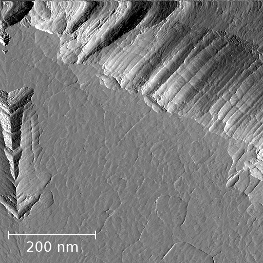
I’m making some major changes to the Teensy firmware and wanted to share this image of a gold surface I took after making some improvements to the way the scan is generated. Previously, I was just advancing the scan in single pixels increments, but this produced relatively coarse motion which seemed to be causing spikes in the tunneling current during scanning, and possibly exciting scanner resonances.
I’m now advancing the scan in much smaller increments to provide smoother scanning motion, and averaging all the data acquired between pixels. So far, the results are looking pretty good! The above image is of the error signal, and it looks quite crisp and clean compared to most of my previous scans. Unfortunately I crashed this tip several times while debugging code, so smaller scans didn’t look quite as good, although I was still able to resolve atomic steps. The roughness in the upper right part of the image is likely the site of a tip crash. The weird mirror-effect on the left edge is due to an off-by-one error in the code somewhere…
I can also run faster scan rates now, up to about 40 Hz at 512 pixels per line, and faster at lower resolutions. This seems to be a little too fast for a disc scanner but should work well with the small tube scanner that I’ll be upgrading to soon. I’ll post the new code I’m working on soon.

Hi, amazing picture!
I was wondering considering the very different texture near the top right, which I don’t believe to be a changed surface due to crashing, but rather some kind of interaction between the tip and the sample. I assume the scanning was horizontally left to right, then next row. observe how roughly the same intensity profile occurs for every line excepted a little earlier each time.
Imagine there there is some kind of (nonconducting) wall going from top left to middle right. Imagine that the tip scans horizontally until in contact with the wall, then as it is forced right, it follows the wall down. So the height of the conducting surface along the wall is retraced for every horizontal scan (horizontal until it hits and follows the wall). This explains why the same intensity profile is present over large vertical distance in the top right corner. Also explains why it is roughly perpendicular to the wall, and irregular by stick slip…
Just speculating though… Not sure what the wall would be to be nonconducting: debris? oil/fat?…
Or perhaps the tip has multiple pointy protrusions, one of which became nonconducting?
the rest of the picture is beautiful!
LikeLike
Hi ludwig,
This is an error-signal image, so it roughly corresponds to the gradient of the topography in the scan direction. Bright areas of the image have a upward slope going from left to right, and dark areas have a downward slope. The height image (not shown here) actually shows a deep pit right in the top-right corner, so it really looks like a tip crash. I definitely crashed the tip more than once while debugging code too.
LikeLike
wow, software post at last?
LikeLike
Haha, yeah I know it’s taking a while, I just don’t have a lot of time to work on this stuff. If you want the old software I can send it to you.
LikeLiked by 1 person